Batch Wafer ID Reader Posted on 26 7 月, 2022 at 7:07 上午.Written by fuxi.deng For 8 inch wafer only. Compact footprint for tabletop use. Alignment & ID reading of various wafer types. Fast cycle times (35 sec / 25 slot). User friendly SEMI standard GUI. CE certified. SEMI standard compliant. No additional Hardware require. 聯絡我們
Wafer ID Reader Posted on 26 7 月, 2022 at 7:06 上午.Written by fuxi.deng Support to decode OCR, Barcode, Data Matrix and QR-code Revolutionary integrated RGB illumination Intelligent recipe handling Fully automatic exposure control Wider FOV 35mm x 13mm Code shift compensation, Flexible ROI Additional external RGB illumination 聯絡我們
Thermal Wafer Chucks Posted on 26 7 月, 2022 at 7:05 上午.Written by fuxi.deng Onsite upgrade. Air cooling. Low running cost. Temperature ranges from -65 to +400 °C. 聯絡我們
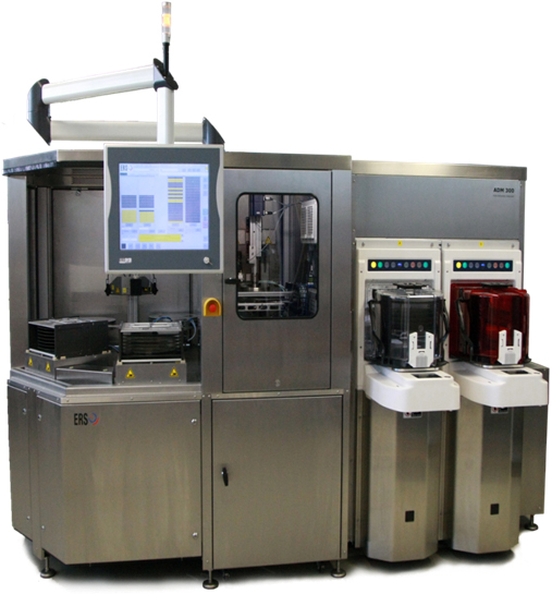
Warpage Adjustment Tool Posted on 26 7 月, 2022 at 7:01 上午.Written by fuxi.deng Fully auto warpage adjust of wafers up to 300mm. Warpage inspection and auto readjust function available. Can be configured for up to 4 FOUP load ports. Wafer ID reading and SECS/GEM comm. Warpage wafer handling ability: up to 7mm. 聯絡我們
Automatic Debonder Machine Posted on 26 7 月, 2022 at 7:01 上午.Written by fuxi.deng Automaic 330/300/200mm eWLB debonding tool. Safe separation of eWLB substrate from its carrier. Throughput-enhancing preparation chamber. Temperature range : +20℃ up to +240℃. Warpage wafer handling ability: up to 7mm. Typical post-warpage adjustment result : up to 500um. 聯絡我們
Thermal Air TA-5000 Posted on 26 7 月, 2022 at 7:00 上午.Written by fuxi.deng 50 / 60Hz same system. Features: Continuous Air Flow up to 18 SCFM @-80C/+225C -55C to +125C/ +125C to -55C less than 10sec Ultra Stable DC Temperature Control Frost Free Operation/ Built-in Air Dryer No LN2 or CO2 Required Application fields: Device temperature characterization on components, hybrids, modules, PCBs, and other electronic and non-electronic assemblies at precise temperature sensing from - 80°C to + 225°C 聯絡我們
LEDA T200 Posted on 26 7 月, 2022 at 6:56 上午.Written by fuxi.deng Fiber-less. Position Sensor for Filters. Adjustable Test Items. One Step Test for VF , LOP & WLD. Compensate for Multi-Optical. Calibration. 聯絡我們
LEDA A2000P Posted on 26 7 月, 2022 at 6:55 上午.Written by fuxi.deng A2000P is fully auto LED chip inspection system, including: High resolution optical system. Muture analysis logical. Muture and Steady hardware. To verify the defect upon LED chips. 聯絡我們
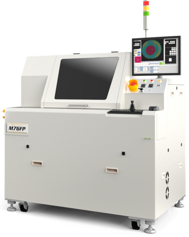
LEDA M76FP Posted on 26 7 月, 2022 at 6:54 上午.Written by fuxi.deng Quickly change bin design. Max 125 bin grade. Single transfer system to load/unload. Auto nozzle clean module(option). Up to 4” wafer sorting with 8” ring. 聯絡我們
Probe Needles Posted on 26 7 月, 2022 at 6:53 上午.Written by fuxi.deng For Probing Provide with below materials: Beryllium-Copper Heat-treat Beryllium-Copper Paliney Alloy series H3C Alloy Tungsten Accept customize spec, including the tip angle, tip radius, or the tip length 聯絡我們